Inside a sealed room in Hsinchu, Taiwan, a machine the size of a city bus is firing droplets of molten tin into a vacuum at 70 metres per second, vaporising each one with a laser, and using the burst of light that erupts to print circuit patterns smaller than a strand of DNA. The light has a wavelength of 13.5 nanometres. It does not occur naturally on Earth’s surface. It is absorbed by air, by glass, by almost everything, which is why the entire optical path has to be held in vacuum and steered with mirrors polished to atomic smoothness. This is how TSMC makes the chips that run the modern world.
The process is called 2-nanometre. It entered volume production in the fourth quarter of 2025, and by the company’s own count, five 2nm fabs are ramping in 2026 — the most aggressive node expansion in TSMC’s history.
What “2 nanometres” actually means
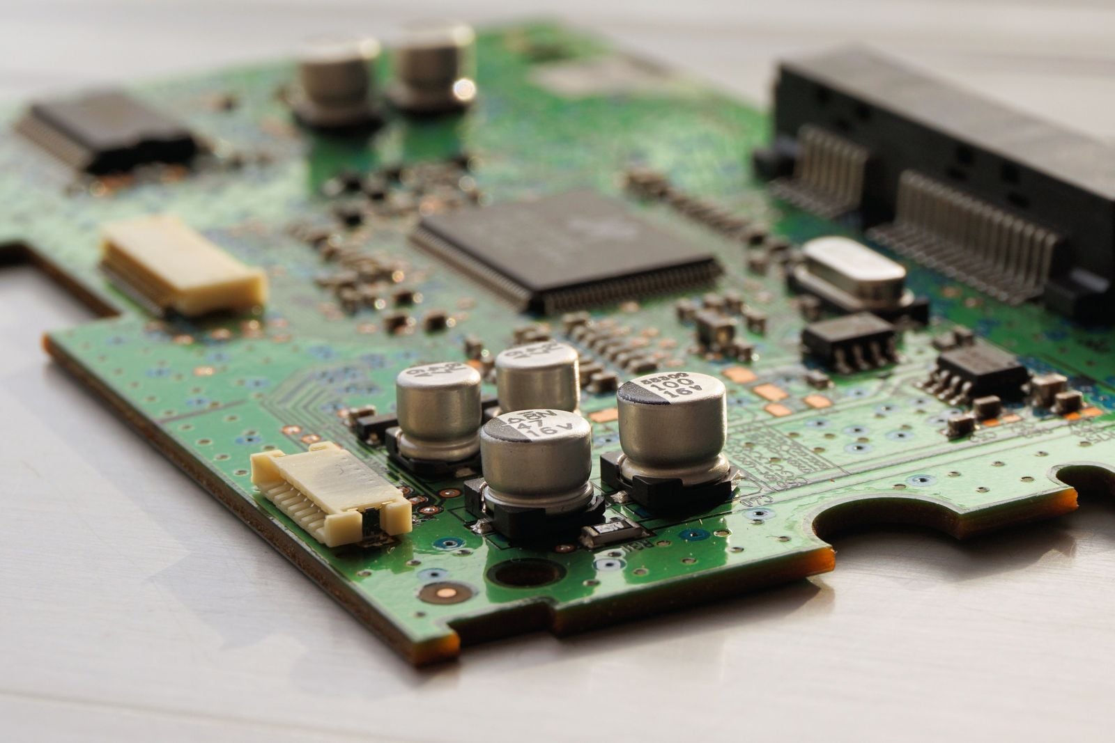
A human hair is roughly 80,000 nanometres across. A red blood cell is about 7,000. The smallest features TSMC is patterning are measured in single-digit nanometres — gate pitches around 45 nm, metal pitches around 20 nm, and individual transistor structures whose narrowest dimensions are a few atoms wide. The “2nm” label is a marketing name inherited from decades of process-node convention; the actual physical feature sizes vary across the chip. The point stands: these are structures roughly 25,000 times finer than the hair on your arm, fabricated by the hundreds of billions on a single wafer.
To print something that small, you need light with a wavelength small enough to resolve it. Visible light — the stuff your eyes use — has wavelengths between 380 and 700 nanometres. Useless. Ultraviolet lithography pushed down to 193 nm using argon-fluoride lasers, and that carried the industry for two decades through clever optical tricks. But at 2nm, even those tricks run out.
The light that doesn’t exist on Earth
Extreme ultraviolet light, at 13.5 nanometres, sits in a part of the electromagnetic spectrum normally found only in the corona of the Sun and in laboratory plasmas. Earth’s atmosphere absorbs it within a few centimetres. You cannot focus it with a lens — every known glass swallows it. You cannot bounce it off an ordinary mirror, because every ordinary mirror absorbs it too.
So ASML, the Dutch company that builds the only EUV scanners on the planet, had to invent a new way to make light. Inside each machine, a tin droplet about 25 micrometres across falls through a vacuum chamber. A pre-pulse laser flattens it into a pancake. A main pulse — a carbon-dioxide laser firing tens of kilowatts — vaporises the pancake into a plasma hot enough to emit at 13.5 nm. This happens 50,000 times per second. The light that pours out is then bounced through a series of mirrors coated with 40 to 50 alternating layers of molybdenum and silicon, each layer just a few atoms thick, tuned so that the reflections from each interface add up constructively. Even then, each mirror reflects only about 70 percent of the EUV that hits it. By the time the light reaches the wafer, after a dozen bounces, most of it is gone.
Why this matters past the fab door
Every leading-edge AI accelerator, every new iPhone processor, every Nvidia datacentre GPU now flowing into hyperscaler clusters traces back to a handful of EUV scanners running in a handful of fabs, almost all of them on a single island. TSMC’s own customers — Apple, Nvidia, AMD, Qualcomm, Broadcom — are queuing for 2nm allocation. At its May 2026 Hsinchu symposium, TSMC executives said AI demand is expanding from cloud datacentres into edge devices, with advanced packaging capacity now the binding constraint as much as raw wafer output.
Taiwan’s dominance in leading-edge logic production represents one of the most concentrated dependencies in modern industrial history. The phrase “silicon shield” — the idea that the rest of the world has too much riding on Taiwanese fabs to let them be disturbed — gets repeated in policy circles in Washington, Tokyo, Berlin and Canberra.
The yield problem, and why it’s getting solved faster than expected
Printing a feature 13.5 nanometres wide is one thing. Printing it billions of times, on hundreds of wafers a day, with defect rates low enough that the resulting chips actually function, is another. Each 2nm wafer goes through more than a thousand individual process steps over roughly three months inside the fab.
The architecture has changed too. At 2nm, TSMC has moved to a gate-all-around nanosheet structure, where the channel through which current flows is wrapped on all four sides by the gate that controls it. This recovers electrostatic control at scales where the older fin design was leaking current like a sieve. The catch is that nanosheets are harder to build. Stacks of silicon and silicon-germanium have to be grown, then the germanium etched out from underneath, leaving suspended ribbons of silicon a few atoms thick.
Even so, TSMC’s 2nm yield learning curve has outperformed 3nm at the equivalent point in its ramp — a result that surprised analysts and pushed the company to accelerate the buildout of its five-fab plan.
Water, power, and the physical cost of a transistor
A single TSMC fab consumes roughly the electricity of a mid-sized city and the water of a small one. Taiwan’s periodic droughts have highlighted the tension between agricultural water use and semiconductor manufacturing, with fabs requiring vast quantities of ultrapure water for wafer rinsing.
The water is not for cooling. It is for rinsing — ultrapure water, filtered to part-per-trillion purity, used to wash wafers after every chemical step. A single 2nm wafer can consume thousands of litres before it leaves the fab.
Then there is the electricity. EUV scanners draw around a megawatt each when running. A modern fab houses dozens of them. The fans that move filtered air through the cleanroom, the pumps that maintain vacuum, the chillers that hold the wafer stage at a constant temperature to within millikelvins — all of it adds up to a facility whose annual power draw rivals a national grid in a small country.
The geopolitics that the physics created
The diplomatic and military temperature around Taiwan has been climbing steadily for years, and the chips are the reason.
Washington has spent the past three years trying to diversify. The CHIPS and Science Act underwrote TSMC’s new fabs in Arizona, where the first phase has begun limited production of older nodes. Samsung is racing to catch up at 2nm in South Korea. Intel is trying to re-enter the foundry business with its 18A node. None of them are yet at TSMC’s volume or yield.
And the next step is already in motion. The race to 1nm has started, with TSMC, Samsung and Intel each publishing roadmaps targeting the second half of this decade. At 1nm — really a marketing label for a node whose physical features will be even smaller than 2nm’s — the industry will likely need High-NA EUV, a next-generation tool from ASML that uses larger mirrors and a numerical aperture of 0.55 to print finer features in a single exposure. Each High-NA machine costs north of $380 million. TSMC has reportedly ordered several.
What a single chip carries
An Apple M-series processor fabricated on TSMC’s 3nm node contains roughly 25 billion transistors on a die about the size of a fingernail. A 2nm successor will likely cross 40 billion. Nvidia’s largest AI accelerators, built on TSMC nodes and stitched together with the company’s CoWoS advanced packaging, push past 200 billion transistors per package.
Every one of those transistors is a switch that can flip on and off billions of times per second, drawing currents measured in nanoamperes, governed by gate oxides only a few atoms thick. The signals that race through them are what trains a large language model, what decodes a video on your phone, what guides a missile, what runs the avionics of an F-35, what handles a credit-card transaction in Frankfurt.
Analysts estimate that a sudden loss of Taiwanese leading-edge output would cost the global economy somewhere in the trillions of dollars in the first year alone, and that no plausible reshoring plan can replace that capacity inside a decade.
The mirror, the droplet, the wafer
Strip away the geopolitics and the dollar figures and what is left is a physical fact that still seems implausible when you say it out loud. A Dutch machine fires a laser at a falling drop of tin, creating a plasma briefly hotter than the surface of the Sun, which emits a flash of light at a wavelength that does not naturally reach Earth’s surface. That light bounces off a series of mirrors smoother than anything else humans have ever polished. It lands on a silicon wafer coated in a chemically tuned resist. The pattern it prints there is the blueprint for a transistor measured in atoms.
This happens 50,000 times a second, inside a vacuum chamber, on an island that lives under the daily possibility of blockade. The chips that come out are then shipped to factories in Malaysia, Vietnam, China, the United States, assembled into phones and servers and satellites, and routed back across the world.
Voyager 1, as covered in earlier Space Daily reporting, is still transmitting from beyond the heliosphere on 22 watts. The probe was built with transistors measured in micrometres — thousands of times larger than what TSMC prints today. The arc from one to the other, in roughly fifty years, traces almost the entire arc of the semiconductor era. The next leap, to 1nm, is already scheduled. The tin droplets are already falling.