| . |  |
. |
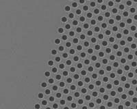
Los Angeles (SPX) Aug 10, 2006 Georgia Tech researchers have found a way to shrink all the sensing power of sophisticated biosensors - such as sensors that can detect trace amounts of a chemical in a water supply or a substance in your blood - onto a single microchip. In compact communication, signal processing and sensing optics technologies, multiple wavelengths of light are combined as a space-saving measure as they carry information. The wavelengths must then be separated again when they reach their destinations. Wavelengths used for these sophisticated applications have very high spectral resolution, meaning the distance between wavelengths is very small. The device that sorts out these crowded wavelengths is called a wavelength-demultipler (WD). Compact optical WDs are key in spectral analysis for biosensers small enough to fit on a chip and for integrated circuits for optical information processing. Georgia Tech researchers have designed a WD able to function at very high resolution in much tighter confines (as small as 64 microns by 100 microns - smaller than a millimeter) by developing a new design for photonic crystals, which are highly periodic structures typically etched in very thin silicon that are designed to control light and have the potential to revolutionize everything from computing to communications. The research had been published in Laser Focus World and Optics Express and was recently presented at the Conference on Lasers and Electro-Optics (CLEO 2006). "We believe we have developed the most compact WD that has been reported to date," said Ali Adibi, a professor in Georgia Tech's School of Electrical and Computer Engineering and the lead researcher on the project. "If you want to have many optical functions on a single micro- or nano-sized chip, you have to be able to practically integrate all those functions in the smallest amount of space possible. Our WD solves many problems associated with combining delicate optical functions in such a small space." The Georgia Tech team was able to shrink its WD by combining into one crystal three unique properties of photonics crystals - the superprism effect (separating wavelengths much more finely than a regular prism), negative diffraction or focusing (reversing the expansion of the light beam and focusing it back to its original size after interacting with the material being analyzed) and negative refraction (filtering wanted and unwanted wavelengths). By combining these effects, Georgia Tech's WD takes an expanded beam of light and instead of expanding it further as wavelengths are separated, focuses the wavelength into different locations. The structure simultaneously separates wavelengths, focuses wavelengths instead of refracting them and then separates the wavelengths in one structure, solving the problems associated with wavelength interference without adding extra devices to the system. "This project really demonstrates the importance of dispersion engineering in photonic crystals - and it's all done by changing the geometry of some holes you etch in the silicon. It's very simple and it allows you to combine properties into one material that you never could before," Adibi said. Despite the more advanced capabilities of the photonic crystals used in Georgia Tech's WD, they are no more complex or difficult to manufacture than conventional photonic crystals, Adibi added. The team members created these newly optimized crystals by using a modeling tool they developed two years ago to test the properties of a material much faster than time-consuming conventional numerical methods. The result is a WD that is less than a millimeter in all dimensions rather than the several centimeters of other currently available WDs. Furthermore, Georgia Tech's WD can be integrated for several other functionalities on a single chip for signal processing, communications, or sensing and lab on-a-chip applications. The work was supported by the Air Force Office of Scientific Research (AFOSR, G. Pomrenke) and in part by the National Science Foundation (NSF) and David and Lucile Packard Foundation. Related Links Georgia Tech All about the technology of space and more
 Washington DC (SPX) Jul 27, 2006
A chemical alloy, used in everyday electronic items such as rewritable CDs and DVDs, serves as the source of a new computer chip which researchers hope will demonstrate non-volatile memory, or information storage retention without a power source, in the radiation-hardened space environment. |
|
| The content herein, unless otherwise known to be public domain, are Copyright 1995-2006 - SpaceDaily.AFP and UPI Wire Stories are copyright Agence France-Presse and United Press International. ESA PortalReports are copyright European Space Agency. All NASA sourced material is public domain. Additionalcopyrights may apply in whole or part to other bona fide parties. Advertising does not imply endorsement,agreement or approval of any opinions, statements or information provided by SpaceDaily on any Web page published or hosted by SpaceDaily. Privacy Statement |