| . |  |
. |
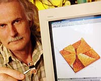
Washington DC (SPX) Apr 17, 2006 A study of how electrons behave in circuitry made from ultrathin layers of graphite ďż˝ known as graphene ďż˝ suggests the material could provide the foundation for a new generation of nanometer scale devices that manipulate electrons as waves ďż˝ much like photonic systems control light waves. In a paper published April 13 in Science Express, an online advance publication of the journal Science, researchers at the Georgia Institute of Technology and the Centre National de la Recherche Scientifique (CNRS) in France report measuring electron transport properties in graphene that are comparable those seen in carbon nanotubes. Unlike carbon nanotubes, however, graphene circuitry can be produced using established microelectronics techniques, allowing researchers to envision a "road map" for future high-volume production. "We have shown that we can make the graphene material, that we can pattern it, and that its transport properties are very good," said Walt de Heer, a professor in Georgia Tech's School of Physics. "The material has high electron mobility, which means electrons can move through it without much scattering or resistance. It is also coherent, which means electrons move through the graphene much like light travels through waveguides." The results should encourage further development of graphene-based electronics, though de Heer cautions that practical devices may be a decade away. "This is really the first step in a very long path," he said. "We are at the proof-of principle stage, comparable to where transistors were in the late 1940s. We have a lot to do, but I believe this technology will advance rapidly." The research, begun by de Heer's team in 2001, is supported by the U.S. National Science Foundation and the Intel Corporation. In their paper, the researchers report seeing evidence of quantum confinement effects in their graphene circuitry, meaning electrons can move through it as waves. "The graphene ribbons we create are really like waveguides for electrons," de Heer said. Because carbon nanotubes conduct electricity with virtually no resistance, they have attracted strong interest for use in transistors and other devices. However, the discrete nature of nanotubes ďż˝ and variability in their properties ďż˝ pose significant obstacles to their use in practical devices. By contrast, continuous graphene circuitry can be produced using standard microelectronics processing techniques. "Nanotubes are simply graphene that has been rolled into a cylindrical shape," de Heer explained. "Using narrow ribbons of graphene, we can get all the properties of nanotubes because those properties are due to the graphene and the confinement of the electrons, not the nanotube structures." De Heer envisions using the graphene electronics for specialized applications, potentially within conventional silicon-based systems. "We have shown that we can interconnect graphene, put current into it, and take current out," he said. "We have a very promising electronic material. We see graphene as a platform, a canvas on which we can work." De Heer and collaborators Claire Berger, Zhimin Song, Xuebin Li, Xiaosong Wu, Nate Brown, Tianbo Li, Joanna Hass, Alexei Marchenkov, Edward Conrad and Phillip First of Georgia Tech and Didier Mayou and Cecile Naud of CNRS start with a wafer of silicon carbide, a material made up of silicon and carbon atoms. By heating the wafer in a high vacuum, they drive silicon atoms from the surface, leaving a thin continuous layer of graphene. Next, they spin-coat onto the surface a photo-resist material of the kind used in established microelectronics techniques. Using electron-beam lithography, they produce patterns on the surface, then use conventional etching processes to remove unwanted graphene. "We are doing lithography, which is completely familiar to those who work in microelectronics," said de Heer. "It's exactly what is done in microelectronics, but with a different material. That is the appeal of this process." Using electron beam lithography in Georgia Tech's Microelectronics Research Center, they've created feature sizes as small as 80 nanometers. The graphene circuitry demonstrates high electron mobility ďż˝ up to 25,000 square centimeters per volt-second, showing that electrons move with little scattering. The researchers expect to see ballistic transport at room temperature when they make structures small enough. So far, they have built an all graphene planar field-effect transistor. The side-gated device produces a change in resistance through its channel when voltage is applied to the gate. However, this first device has a substantial current leak, which the team expects to eliminate with minor processing adjustments. The researchers have also built a working quantum interference device, a ring-shaped structure that would be useful in manipulating electronic waves. The key to properties of the new circuitry is the width of the ribbons, which confine the electrons in a quantum effect similar to that seen in carbon nanotubes. The width of the ribbon controls the material's band-gap. Other structures, such as sensing molecules, could be attached to the edges of the ribbons, which are normally passivated by hydrogen atoms. Beyond coherence and high electron mobility, the researchers note that the speed of electrons through the graphene is independent of energy ďż˝ just like light waves. The electrons also possess the properties of Dirac particles, which allow them to travel significant distances without scattering. Among the challenges ahead is improving the techniques for patterning the graphene, since electron transport is affected by the smoothness of edges in the circuitry. Researchers will also have to understand the material's fundamental properties, which could still contain "show-stoppers" that might make the material impractical. De Heer has seen hints that graphene may offer some surprises. "We already have indications of some new and surprising electronic properties of this material," he said. "It is doing things that we have never seen in two-dimensional materials before." Graphics: Photographs of researchers with laboratory equipment, scanning electron microscope images of graphene circuitry, prototype graphene device.
Related Links Science Express
 Bethesda MD (SPX) Apr 17, 2006
Iridium Satellite, KDDI Network and Solutions and Pioneer Navicom jointly announce the completion of successful air trials and initial deployment of an automatic helicopter tracking system by the Japanese Fire and Disaster Management Agency. |
|
| The content herein, unless otherwise known to be public domain, are Copyright 1995-2006 - SpaceDaily.AFP and UPI Wire Stories are copyright Agence France-Presse and United Press International. ESA PortalReports are copyright European Space Agency. All NASA sourced material is public domain. Additionalcopyrights may apply in whole or part to other bona fide parties. Advertising does not imply endorsement,agreement or approval of any opinions, statements or information provided by SpaceDaily on any Web page published or hosted by SpaceDaily. Privacy Statement |